Zero ASIC ·
Lowering the Barrier to Chiplets
Chiplets are all the rage these days, even making MIT Technology Review’s 10 Breakthrough Technologies of 2024. This is pretty incredible for such a niche technology! Unfortunately, as of today chiplets are only accessible to semiconductor mega-corps. To unlock the true power of disaggregated chiplet innovation, we need to drastically reduce the barriers to chiplet based design.
One of the barriers to chiplets is the high cost and complexity of die-to-die interfaces. Existing die-to-die electrical interfaces (eg. AIB, UCIe, BoW) are designed to be simple, yet the cost of implementation (or procurement) has remained prohibitive. For chiplets to really take off, we need chiplet interfaces that are small, cheap, and fast.
To this end, we have created a low complexity (and low cost) prototype implementation of the UCIe standard, suitable for a wide range of technology nodes. The interface was designed and simulated entirely using open source EDA tools.
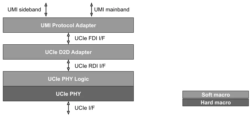
Interface Features
- UCIe specification (v1.1)
- Raw mode
- 16b wide
- Up to 8GT/s maximum
- Tightly coupled mode only
- Designed to UCIe FDI and RDI interface specifications
- Universal Memory Interface protocol
- Simulated using open source tools (Verilator, Xyce, Icarus, and Switchboard).
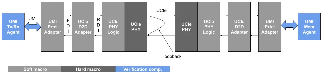
Digital simulation setup
The top level testbench was developed in Python using Switchboard, an open-source high-performance co-simulation library developed by Zero ASIC. Switchboard has built in Python bindings for UMI transactions, making it easy to create test pattern generators and unit tests. The Switchboard library was used to interface with the Verillator simulator to test/simulate the interface in a number of modes, including loopback mode and back-to-back phy-to-phy connections with a UMI memory device on the remote side.
Analog simulation setup
The UCIEe PHY was implemented in GlobalFoundries GF12LP process node and verified using the open-source Xyce simulator. In addition to purely analog simulations, we ran mixed-signal simulations combining PHY RTL with transistor-level analog components. These mixed-signal simulations used the Switchboard get() and put() functions to read and write analog signals from an RTL simulation, leveraging XyceCInterface and VPI/DPI.
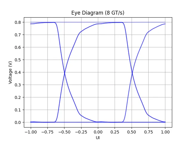
PHY Channel Simulation
The eye diagram below was measured by running an analog simulation of a signal chain consisting of a TX predriver, a TX driver with impedance control, TX and RX pad capacitance, and a lossy channel model based on S parameter data from the UCIe organization. Simulation results were parsed using Spyci and formatted into an eye diagram with NumPy and Matplotlib. We will add more effects to the eye diagram simulation as the design progresses, including power supply noise, crosstalk, and jitter.
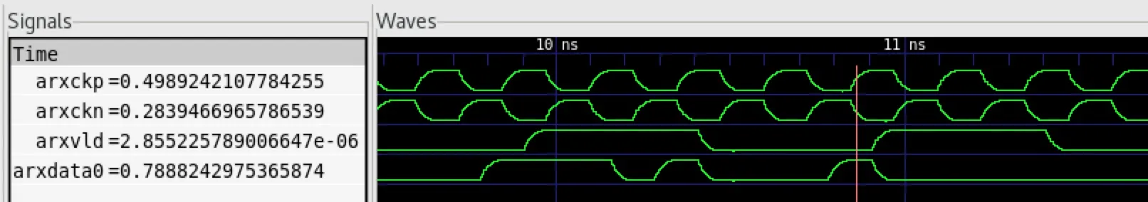
We have also run mixed-signal simulations to check the interaction between low-level PHY circuits and higher-level RTL. The waveforms below show the byte 0x8B being transferred, measured at the receiver end of the channel.
Protocol Layer Simulation
End-to-end transmission was simulated in both loopback and back to back modes. The test follows UCIe spec initialization phase starting with link initialization over sideband, followed by the protocol layer moving to active state and running UMI traffic over the UCIe link. In addition to that the test also demonstrated UMI sideband read/write to the D2D and PHY registers and mailbox read/write. The transactions were checked for data integrity end-to-end.
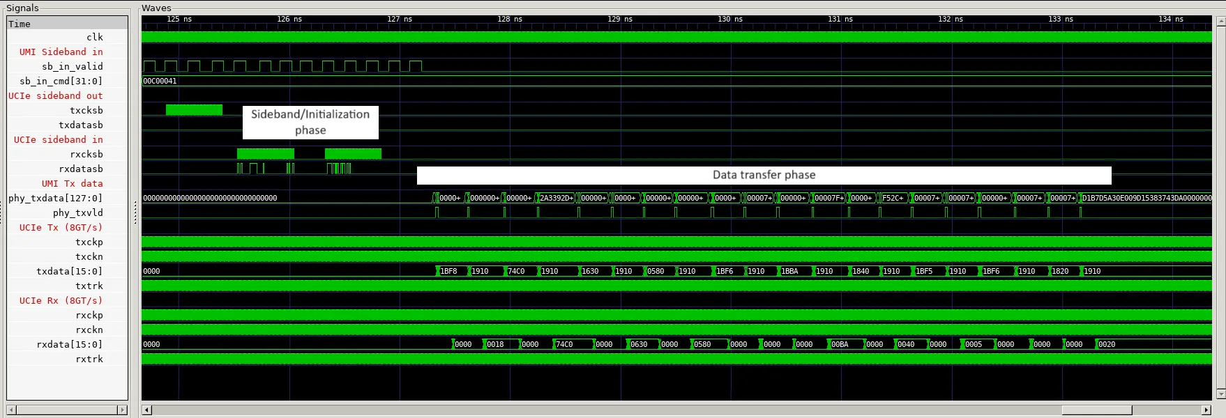
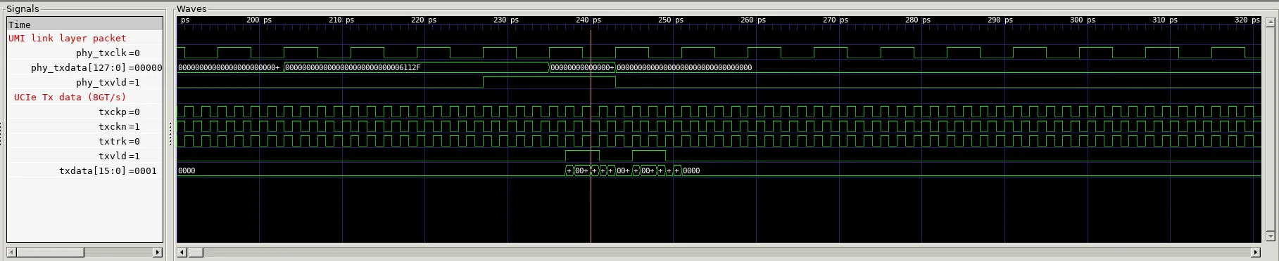
Zooming in on the data phase shows the conversion from 1GHz, 128b wide UMI link layer data to UCIe, 16b, 8GT/s.
References
- UCIe: https://www.uciexpress.org/
- UMI: https://github.com/zeroasiccorp/umi
- Switchboard: https://github.com/zeroasiccorp/switchboard
- Verilator: https://www.veripool.org/verilator/
- Icarus: https://github.com/steveicarus/iverilog
- Xyce: https://xyce.sandia.gov/